In order to accelerate the mass production of solution processed OLED?
At the latest OLED technology trends seminar organized by UBI Research in Seoul COEX on April 26th, professor Seo presented about the status of solution processed OLED for large-area TV production.

Professor Seo emphasized that there are four technical challenges to advance the mass production of solution processed OLED.
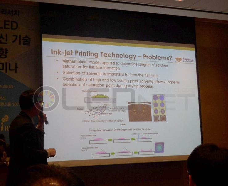
The first challenge is the development of materials that can form stable and flat thin films. When the emitting material for solution process is applied, the solvent causes a convection phenomenon due to solubility and boiling point. Therefore, it is difficult to make a flat film because the speed at which the solvent flows is different for each region.
The second is the development of cross linked HTL materials. Emitting material companies are mixing cross-linking agents into HTL materials for solution process to solve intermixing problems between layers. However, a pinhole is formed due to a cross linking reaction with the surrounding small molecular materials when crosslinked materials in small molecule type are used. This kind of pinhole lowers the uniformity of the thin film, and therefore it is necessary to develop crosslinked HTL materials that can improve the reproducibility and lifetime of OLED in solution process.
The third is the jetting condition. He proposed a jetting condition that can minimize the volume deviation of the emitting material for solution process every head since it is necessary to drop the emitting material for solution process of less than 4 pl to the desired position in the size of 20-50 um to realize 8K. Lastly, he commented that it is required to optimize the drying process of solvent. UBI Research described that the solution OLED process has a simple (5 layer) structure and high material utilization efficiency compared to the conventional deposition process. In addition, it is possible to manufacture large-area OLED with RGB structure without the division of mother glass at Gen8 or higher. When major panel makers adopt solution process, it is available to reduce the manufacturing cost of OLED due to the decrease of equipment and equipment scale as well as material cost and labor cost reduction. According to the 2018 Annual OLED Display Industry Report and 2018 Emitting material Industry Report published by UBI research, solution processed OLED is to be mass produced from 2019 in earnest, and the shipment is expected to be 0.2 million units in 2019 and 9.2 million units in 2022. Accordingly, the emitting material market for solution process is estimated to grow to US$ 110 million in 2022 from US$ 9 million in 2019.
댓글을 남겨주세요
Want to join the discussion?Feel free to contribute!