유비리서치, 2025년 OLED 발광재료 시장 22.5억 달러 전망

OLED 시장 조사 전문 업체인 유비리서치(www.ubiresearch.com)는 최근 발간한 ‘2021년 2분기 OLED 발광재료 마켓트랙’을 인용하며, OLED용 발광재료 시장이 연평균 9%의 성장률로 2025년에는 22.5억 달러 규모를 형성할 것이라고 전망했다.


국가별로 살펴보면, 중국 패널 업체들의 라인 증설에도 불구하고 한국 패널 업체들이 OLED 발광재료 시장을 계속 주도할 것으로 보인다.

한국 패널 업체들의 발광재료 구매액은 연평균 5.8% 증가하여 2025년에는 16.1억 달러에 달할 것으로 보이며, 이는 전체 시장의 71.6% 규모이다. 또한, 향후 5년 동안 한국 패널 업체들의 발광재료 총 구매액은 전체의 72.4%를 차지할 것으로 예상된다. 이에 비해, 중국 패널 업체들의 재료 구매액은 연평균 8.7%의 성장률로 2025년에는 6.4억 달러가 될 것으로 전망된다.

패널 업체별로는, 삼성 디스플레이가 향후 5년동안 43.5%의 점유율로 가장 많이 발광재료를 구매할 것으로 전망되며, LG 디스플레이가 28.9%, BOE가 17.5%를 구매할 것으로 예상된다.

마지막으로 증착 방식별로 살펴보면, RGB OLED용 발광재료가 전체 시장의 78%의 비율을 차지하고WRGB OLED용 발광재료는 20.4%의 비율을 차지할 것으로 예상된다. 올해 하반기에 출시될 것으로 예상되는 삼성 디스플레이의 QD-OLED용 발광재료는 패널 출하량이 많지 않을 것으로 예상됨에 따라, 전체 재료 시장에서2% 미만의 비중을 차지할 것으로 분석된다.


[IMID 2018] LG Display, 수명을 개선한 자동차용 OLED로 2 stack RGB OLED 선보여

829일 부산 BEXCO에서 열린 IMID 2018에서 LG Display의 김관수 연구위원(research fellow)은 자동차용 디스플레이에 적용될 새로운 OLED 기술에 대해 발표했다.

김 연구위원은 현재 모바일 기기에 적용되고 있는 RGB OLEDTV에 적용되고 있는 WRGB OLED는 수명 측면에서 고객사들의 요구를 만족시키지 못하고 있기 때문에, 이를 해결하기 위한 방법으로 RGB OLEDWRGB처럼 tandem 구조를 갖는 2 stack RGB OLED를 소개했다.

2 stack RGB OLED는 다층구조에 CGL(charge generation layer) 층이 더해져 두께가 두꺼울 수 있기 때문에 HTL을 기존보다 얇게 만들고 발광층의 charge balance를 최적화하였다.

그 결과 1 stack RGB OLED보다 1.5배에서 2배 향상된 발광효율과 함께 수명이 T80 기준으로 4배 이상 증가하는 효과가 나타났다고 보고했다.

하지만 2 stack 구조는 일반 구조에 비해 소비 전력이 높은 단점이 있어 이를 해결하기 위한 노력이 필요하다고 지적했다.

초고화질 해상도(UHD)의 OLED 스마트폰 시대 열릴까

최근 스마트폰 기기를 통한 VR 컨텐츠 체험이 증가하는 추세로 인해 고해상도 스마트폰이 요구되고 있으나, 2014년 Galaxy Note4에 최초로 QHD OLED가 적용된 이후 3년 동안 OLED 스마트폰의 해상도는 여전히 QHD급에 머물고 있다.

OLED 스마트폰의 해상도를 결정하는 핵심은 발광층의 증착 공정이다. 현재 적용 되고 있는 상향식 증착 방식은 기판과 FMM(fine metal mask)를 수평으로 하여 증착 장비 상부에 배치한 뒤 하부의 리니어 소스에서 유기물을 증발시켜 RGB 발광층을 형성하는 방식이다.

UHD급 이상의 고해상도 OLED를 제조하기 위해서는 15um 두께 이하의 얇은 FMM이 필요하나 FMM이 얇아질수록 patterning, 인장, 용접등의 기술적인 이슈가 발생하여 양산적용이 어렵다.

이러한 문제들을 극복하기 위해 수직형 증착과 면소스 증착, 다양한 metal mask patterning 기술들이 개발되고 있다.

기판과 FMM를 수직으로 배치하는 수직형 증착기는 일본의 Hitachi에서 최초로 개발하였으며,  Canon tokki도 Finetech Japan 2013에서 6세대 수직 증착 방식의 장비를 공개한바 있으나 현재 양산에 적용되고 있진 않다.


<Finetech Japan 2013에서 공개 된 Canon tokki의 Gen6 vertical type evaporator>

하지만 최근 전자신문에 따르면 Applied Materials에서 6세대 flexible OLED용 수직 증착 방식의 증착 장비를 개발했다고 밝혔으며, 일본의 Japan Display에서 test 중이라고 언급한바 있다.

리니어소스가 아닌 면소스를 이용한 증착 방식도 검토되고 있다. 면소스 증착 방식은 유기물을 금속면에 1차로 증착하여 면소스를 만든 후, 이를 재증발시켜 기판에 유기물 박막을 형성하는 원리로써 지난 iMiD 2017에서 OLEDON의 황창훈 대표는 면소스 증착 방식을 통해 2250 ppi의 고해상도 OLED 구현이 가능하다고 언급하였다.

Metal Mask patterning 기술로는 전주도금(electro forming)과 laser patterning 기술이 주로 거론되고 있다. 전주도금 방식은 Wave Electornics와 TGO Technology, Athene등의 업체에서 개발하고 있으며, laser patterning 기술은 AP Systems에서 개발중에 있다.

이처럼 다양한 관점에서 진행되고 있는 고해상도 OLED 구현을 위한 개발이 현재의 문제를 극복하고 OLED 스마트폰의 UHD 해상도 구현에 기여할 수 있을지 많은 관심이 집중되고 있다.

<OLEDON사가 개발한 면소스 증착 기술 원리>

Is there possibility of High resolution(UHD) OLED Smart-phone generation?

Recently VR contents experience through smart-phone device has been increased, therefore high resolution of smart phone is becoming necessary. However, OLED smart-phone resolution still remains at QHD level for 3 years since QHD OLED is applied to Galaxy Note 4 for the first time in 2014.

The core point that decides resolution of OLED smart-phone is evaporation process for emission layer. Bottom-up type evaporation method, which is applied to the recent devices is that substrate and FMM (fine metal mask) are horizontally arranged on the upper side of evaporator and vaporize the organic material from the lower linear source in order to form RGB layer.

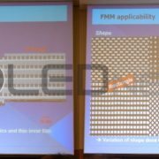
Thin FMM measures less than 15um thick is necessary for making high resolution OLED like UHD level, however, as FMM gets thinner, it would be difficult to make mass production because technical problems will be occurred such as patterning, sealing and welding.

In order to solve these problems, various metal mask patterning technologies are being developed such as vertical type evaporation and plane source evaporation.

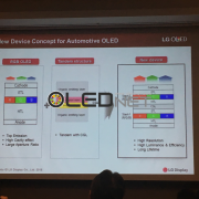
Vertical type evaporator that arranges board and FMM vertical is developed by Hitachi of Japan for the first time. And Canon Tokki exhibited Gen6 vertical type evaporator at Finetech Japan 2013, however it is not being used for mass production at the moment.

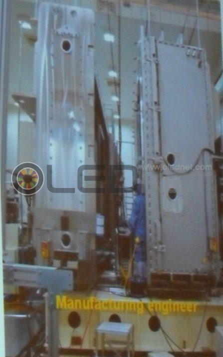
<Canon Tokki’s Gen6 vertical type evaporator which is exhibited at Finetech Japan 2013>


According to the recent ETNEWS, Applied Materials developed Gen6 flexible OLED vertical type evaporator and it is being tested in Japan Display.

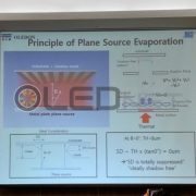
Plane source evaporator is being tested but also the linear source type. Plane source evaporator method is that an organic material is first evaporated on the metal surface to produce plane source, then re-evaporated in order to form an organic thin film on the substrate.

In the past iMiD 2017, representative of OLEDON, Chang Hoon Hwang mentioned that 2250 ppi resolution OLED can be implemented through plane source evaporator.

For metal mask patterning technology, electro forming and laser patterning technology is highlighted. Electro forming method is developed by Wave Electronics, TGO Technology, Athene and so on. Laser patterning technology is being developed by AP Systems.

As such, development for high resolution OLED is receiving great attention whether it can solve the current problems and contribute to UHD resolution implementation for OLED smart-phone.

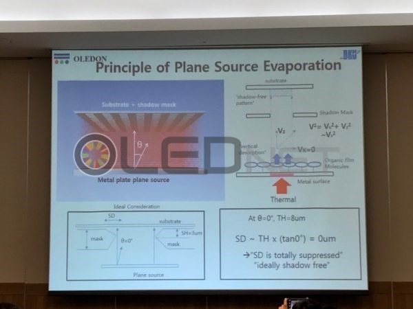
<Principle of plane source evaporation developed by OLEDON>

[iMiD 2017] AP Systems, USPL을 통해 FMM의 해답을 찾다

28일 부산 BEXCO에서 개최된 iMiD 2017에서 AP Systems는 USPL(ultra-short pulse laser)로 1000ppi FMM개발에 성공했다고 발표하였다.

FMM은 화소와 RGB 유기물을 증착하는 역할을 하기 때문에 FMM은 OLED의 해상도와 수율을 결정짓는 요소로서 작용된다. 현재 FMM은 주로 전주(etching) 방식으로 제작되고 있다. 이 방식은 미세 패턴의 정밀도와 두께, 무게에 의한 섀도우 현상이 발생하는 문제가 있어, 이를 해결하기 위해 laser 가공, 전해주조(electro-forming)등 다양한 FMM 제조 공정이 개발되고 있다.

이 중 laser 가공 방식은 laser 조사 시 발생하는 열(thermal effect)로 인해 pin-hole 주변에 burr가 형성되는 이슈가 있다. 이러한 burr는 FMM의 섀도우 구간을 증가, RGB 유기물 증착 시 패턴이 겹치는 현상을 야기시킴으로써 OLED의 해상도를 저하시킨다.

AP Systems는 이러한 점을 착안해 burr 현상이 없고, 나아가 taper angle을 제어하는 burr-free laser process을 개발하였다.

Burr-free laser process는 단방향 펄스를 일정 횟수로 나누어 짧게 조사하는 방식으로 연속적으로 laser를 조사하지 않기 때문에 축적되는 열 에너지가 최소화 되어 burr 형성을 막는다. 또한, laser의 energy를 제어함으로써 energy 축적하여 taper를 형성하는 방식이다.

AP Systems는 이 방법을 통해 ‘1170ppi의 FMM 뿐만 아니라 미세 pin-hole의 모양이 사각형 또는 다이아몬드, 다각형 등 다양한 형태를 갖는 FMM도 제작하였다’며 ‘USPL 방식이 적용된 대면적 FMM 제조 장비도 개발하였다’고 설명하였다.

또한, AP Systems는 FMM 제조 장비에 대해 ‘multi-beam과 USPL이 장착되어 있어 생산성을 향상시킬 수 있으며, UHD를 구현할 수 있다’고 덧붙였다.

14년 Galaxy Note4 출시 이후부터 아직까지 OLED의 해상도는 QHD 급에 머물고 있다. 고해상도(UHD급 이상)를 가지는 OLED를 제조하기 위해서는 FMM이 기술적으로 직면하고 있는 다양한 문제를 해결해야 되는 실정이다. 이에 따라 AP Systems의 USPL 기술이 향후 OLED 시장에 어떠한 영향을 미칠지 앞으로의 귀추가 주목된다.

<AP Systems가 제작한 1000ppi FMM>


<다양한 형태의 FMM>

[iMiD 2017] AP Systems, Find FMM answers through USPL

At iMiD 2017 in BEXCO, Busan on 28th, AP Systems announced that it succeeded in developing 1000ppi FMM with USPL (ultra-short pulse laser).

Since FMM plays a role of depositing pixels and RGB organic materials, FMM serves as a factor that determines resolution and yield of OLED. At present, FMM is mainly manufactured by etching method. This method has a problem that a shadow phenomenon due to the precision, thickness, and weight of the fine pattern occurs, in order to solve this problem, various FMM manufacturing processes such as laser processing and electro-forming have been developed.

Among these, laser processing method has an issue of forming burrs around pin-holes due to the thermal effect caused by laser irradiation. These burrs increase the shadow interval of the FMM, which causes overlapping of patterns during RGB organic deposition, thereby degrading the resolution of the OLED.

AP Systems has developed a burr-free laser process that does not have burr phenomenon and further controls the taper angle.

The Burr-free laser process is a short-time irradiation of unidirectional pulses at a constant number of times, since the laser is not continuously irradiated, it minimizes accumulated heat energy and prevents burr formation. In addition, by controlling energy of the laser, it accumulates energy and forms taper.

In this way, AP Systems explained ‘they produced FMM with various shapes of fine pin-holes such as square, diamond, and polygonal shapes, as well as 1170ppi FMM’, and ‘’We also developed large-area FMM manufacturing equipment with USPL method’.

AP Systems also added ‘multi-beam and USPL is equipped for FMM manufacturing equipment so that it can improve productivity and realize UHD’.

Since the launch of the Galaxy Note4 in 2014, the OLED resolution has remained at the QHD level yet. In order to manufacture an OLED having a high resolution (UHD level or higher), it is necessary to solve various technical problems faced by FMM. Accordingly, it is noteworthy how USPL technology of AP Systems will affect the future OLED market.

<1000ppi FMM produced by AP Systems>


<various type of FMM produced by AP Systems>


Developing ultra-definition display with a color filter technology

A color filter technology has been developed that can bring forward commercialization of next generation’s TVs with ultra-definition visibility and lower prices. The National Research Foundation of Korea (a chairman of the board, Moo-jae, Cho) announced that Prof. for Korea University, Byeong-kwon, Joo’s research team has developed a complementary plasmon color filter having sharp display and high resolution. The color filters which are currently used in the display industry mainly are optical absorption type using pigments or dyes. It has low chemical stability since it is based on organic materials and high unit cost due to manufacturing RGB filters separately. On the other hand, the optical interference type plasmon color filter using inorganic materials can simultaneously produce various color filters at low cost, but there is a problem that the color purity is in decline due to color interference occurring in the two-dimension array of nanostructures.

<Transmittance spectrum according to opening ratio of Hole pattern and dot pattern structures, Source: The National Research Foundation of Korea>

The research team applied a reversal approach to break out the existing pattern as complementary design method that combines dot pattern with hole pattern. It is a general viewpoint of academia that it is difficult to apply dot pattern to a transmission color filter in the form of reversing the existing hole pattern. However, the team assured that the extraction of high purity for red is possible through effective blocking the leakage of short wavelengths by dot pattern under certain conditions. The result is shown that the range of implementing color in the complementary designed plasmon color filter is widened over 30% than before.

<Plasmonic color filter of Hole pattern and Dot pattern structure produced, Source: The National Research Foundation of Korea>

In addition, the implementing of various color of the complementary plasmon color filters is available such as red, green, and blue by adjusting only the geometric parameters of the nanopattern. The performance can be improved without additional costs since the existing materials and manufacturing methods could be used as usual.

Prof. Byeong-kwon, Joo explained that “This research has developed a plasmon color filter with high color reproducibility through a complementary design method. This is expected to accelerate the development of the next-generation display combining nano-optic devices.”

The research results were performed by supporting of the Basic Research Support Project(private research) of the National Research Foundation of Korea at the Ministry of Science, ICT and Future Planning, the Ministry of Education·BK21 support project of the National Research Foundation. It was published in the Scientific Reports affiliated journal of an international journal Nature, on January, 13th.

초고화질 디스플레이 컬러필터 기술 개발

초고화질 선명도를 가지면서도 가격은 더욱 저렴한 차세대 TV 상용화를 앞당길 수 있는 컬러필터 기술이 개발되었다. 한국연구재단(이사장 조무제)은 주병권 교수(고려대) 연구팀이 선명하고 해상도가 높은 색을 나타낼 수 있는 상보형 플라즈몬 컬러 필터를 개발했다고 밝혔다. 현재 디스플레이 산업에서 주로 사용하는 컬러필터는 안료나 염료를 이용한 광흡수 방식이다. 이는 유기재료를 기반으로 하기 때문에 화학적 안정성이 낮고, RGB 필터를 각각 제조해야 하기 때문에 단가가 높다. 반면 무기재료를 사용하는 광간섭 방식의 플라즈몬 컬러필터는 저렴한 비용으로 다양한 색의 필터를 동시에 제조할 수는 있으나, 나노 구조물의 이차원 배열에서 발생하는 색의 간섭 현상 때문에 색 순도가 저하되는 문제점이 있다.

<Hole(음각) 패턴과 dot(양각) 패턴 구조의 개구 비율에 따른 투과 스펙트럼, 출처 : 한국연구재단>

연구팀은 음각 패턴에 양각 패턴을 조합하는 상보형 설계방법으로 기존의 정형화된 패턴 모양을 탈피하는 역발상을 적용했다. 양각 패턴은 기존의 음각 패턴을 반전시킨 형상으로 투과형 컬러필터에 응용하기 어렵다는 것이 학계의 일반적인 시각이었다. 그러나 연구팀은 특정 조건에서 양각패턴이 단파장의 누설을 효과적으로 차단함으로써 순도 높은 적색 추출이 가능함을 확인했다. 그 결과, 상보형으로 설계된 플라즈몬 컬러필터에서 색을 구현하는 영역이 이전보다 30% 이상 넓어지는 결과를 확인할 수 있었다.


<제작된 Hole(음각) 패턴과 dot(양각) 패턴 구조의 플라즈모닉 컬러필터, 출처 : 한국연구재단>


또한 상보형 플라즈몬 컬러필터는 나노 패턴의 기하학적 변수만 조절하면 적색, 녹색, 청색 등 다양한 색상 구현이 가능하다. 기존의 재료와 제조 방법을 그대로 사용할 수 있기 때문에 추가적인 비용 발생 없이 성능을 향상시킬 수 있다.


주병권 교수는“이 연구는 상보형 설계 방법을 통해 높은 색재현성의 플라즈몬 컬러필터를 개발한 것이다. 이 연구가 나노광학소자를 결합시킨 차세대 디스플레이의 개발을 앞당기는 계기가 될 것으로 기대된다.”라고 연구의 의의를 설명했다.


이 연구성과는 미래창조과학부 한국연구재단의 기초연구지원사업(개인연구), 교육부·한국연구재단의 BK21지원사업 등의 지원을 받아 수행되었다. 국제적인 학술지 네이처(Nature) 자매지인 사이언티픽 리포트(Scientific Reports) 1월 13일자에 게재되었다.


[IFA2016] Where Does the Confidence of LG Electronics Come From?

LG Electronics has displayed OLED TV on about half of the entire IFA2016 exhibition’s space, overwhelming the whole area.

160902_1

160902_2

160902_3

160902_4

There is no need for words. You just have to enjoy the exhibition with your eyes.

160902_5

Apart from the image quality, LG promoted its slim product design by the expression “Picture on glass.”
There is no need for words. Exhibition is enough to show why OLED TV is better than LCD TV.

In the previous CES2016, LG Electronics booth was as dark as a movie theater. Presumably, it wanted to show the strength of OLED TV, “black”, well but it could rather be seen as a product that functions properly only in the dark.

CES2016 LG Electronics Booth: The light was as dark as a movie theater

CES2016 LG Electronics Booth: The light was as dark as a movie theater

However, the difference becomes definite when we compare the ceiling light of CES2016 and the light of IFA2016. It became brighter indeed. LG Electronics has changed.

It became confident enough to highlight merits of OLED TV even in a bright area. OLED panel structure of TV produced by LG Display has changed from bicolor structure laminated with three layers of B (blue) and YG (yellow-green) to a three-layers structure that uses B, R, and G to realize three colors. The efficiency and brightness of the colors have become overwhelmingly outstanding.

LG is not the son of darkness anymore. Through the exhibition, it expressed its confidence to have secured the quality to contend with LCD TV.

Of course, it also indicated to continue LCD TV business. It displayed LCD TV, which applied QD technology, in one side so that it’s not compared with numerous OLED TVs. The exhibition of LCD TV, positioned in the corner after losing power, shows that the time is getting closer for competitors to wake up from the illusion that LCD TV will last forever.

160902_7

삼성 ” RGBW 4K 해상도 논란 일단락”…ICDM서 “TV 해상도 측정시 화질 선명도 값 명시” 결론

RGB – RGBW 비교 이미지.(출처=삼성전자)

강현주 / jjoo@olednet.com

지난 24일(현지시간) 미국 샌프란시스코에서 개최된 ICDM (국제 디스플레이 계측위원회, International Committee for Display Metrology) 정기총회에서 그간 4K UHD 해상도 논란을 불러 일으켰던 RGBW 방식 디스플레이 관련 의미 있는 결론을 내렸다고 삼성전자가 26일 주장했다.

TV 디스플레이의 해상도를 측정할 때 기준이 되는 ‘라인(Line)’의 숫자만을 세는 것이 아니라 실제로 디스플레이가 원본 해상도를 얼마나 잘 표현해 낼 수 있는지를 나타내는 ‘화질 선명도(Contrast Modulation)’ 값을 반드시 명시해야 한다는 데 합의한 것이다.

이번 결정은 다양한 TV 디스플레이 방식이 등장함에 따라 보다 정확한 해상도 정보 제공을 위해 기존 측정법을 보완해야 할 필요성에서 출발했다. 기존 측정법에도 ‘화질 선명도’ 평가항목은 있었지만 이를 통과시키는 기준 값이 낮아 해상도 차이를 정확하게 나타내기 어렵다는 점이 지적돼 왔다.

RGBW 방식의 TV 디스플레이는 3,840×2,160의 완전한 UHD 해상도 기준으로 볼 때, 평균 60% 수준의 화질 선명도 값을, RGB 방식의 UHD TV 디스플레이는 평균 95%의 화질 선명도 값을 갖는 것으로 알려져 있다.

기존에는 50%만 넘으면 별도의 표시를 하지 않아도 됐지만, ICDM의 이번 결정에 따르면 앞으로는 화질 선명도 측정값을 반드시 표기해야 한다.

ICDM은 이번 ‘RGBW 방식 디스플레이 해상도 측정 기준 개정안’을 전 세계 화질 전문가와 회원사들이 참석한 가운데 참석인원 3분의 2 이상의 찬성으로 채택했다. 이로써 작년 9월 총회에서 촉발된 4K 해상도 논쟁은 일단락됐다. 지난 2월 회의에서는 기존의 해상도 측정방식이 RGBW 방식의 디스플레이에 적용하기에는 불완전하기 때문에 주의를 요한다는 검토의견을 낸 바 있다.

ICDM의 이번 결정은 소비자들에게 보다 정확하고 구체적인 디스플레이 해상도 정보를 전달할 수 있게 됐다는 데 의의가 있다. 향후 ICDM은 보다 발전한 디스플레이 기술 현실에 맞게 과거의 낮은 화질 선명도 기준은 폐지하고, 실제 화질 차이를 명확히 표현할 수 있도록 해상도 평가법을 최종 보완할 계획이다.

이번 회의에 참석한 세계적인 영상기기 화질 전문가인 조 케인(Joe Kane)은 “업계는 물론 디스플레이 전문가들과의 협력 끝에 디스플레이 해상도의 정확한 정의를 하고 이를 소비자들에게 일관된 방식으로 전달하는 해법을 제시할 수 있었다”고 언급하며, “이로써 소비자들은 시장에 나와 있는 여러 제품들의 사양 차이를 더욱 손쉽게 비교할 수 있을 것이다” 라고 덧붙였다.

한편 ICDM은 1962년 설립된 디스플레이 업계 최고 전문기구인 SID(Society for Information Display) 산하 위원회로, 디스플레이 관련 규격을 제정하고 관련 정보를 제공하고 있다. 디스플레이 관련 분야 전 세계 전문가 250여명과 독일 TUV와 같은 전문 인증 기관, 삼성전자, LG전자, 파나소닉 등 주요 제조사 50개 이상의 회원이 활동 중이다.

유비산업리서치, ‘2015 Display Printed Electronics Seminar’ 개최

  • 국가간 치열한 경쟁의 장이 펼쳐지고 있는 디스플레이 분야에 경쟁력 확보를 위한 인쇄전자 기술을 파악할 수 있는 세미나 장 열려…
  • 유비산업리서치, ‘2015 Display Printed Electronics Seminar’ 개최


최근 디스플레이 분야는 중국의 공격적 투자와 재역전을 노리는 일본 등 국가간 치열한 경쟁이 일고 있다.

이에 한국의 디스플레이 분야 경쟁력 확보를 위해 필수 기술로 떠오르고 있는 인쇄전자 기술에 대해 알아보고 최신 기술 동향을 파악할 수 있는 세미나 장이 마련된다.

‘디스플레이 전문 기업’ 유비산업리서치(http://www.ubiresearch.co.kr, 대표 이충훈)는 10월 07일(수) 서울 서초구에 소재한 The K Seoul Hotel에서 핵심 전문가 집단을 모시고 인쇄전자 기반의 디스플레이에 대한 최신 기술 개발 동향에 대해 다루는 ‘2015 Display Printed Electronics Seminar’를 개최한다고 밝혔다.

인쇄공정 또는 용액공정은 세계적으로 많은 기대를 받고 있는 새로운 제조기술이다. 인쇄전자의 산업화에 대응하기 위해 국제표준기구 IEC에서 설립한 TC119 국제 간사를 맡고 있는 한국생산기술연구원 강경태 인쇄전자 센터장이 ‘Printed Electronics 국제표준 동향 및 산업 전망’이라는 주제로 인쇄전자산업의 현재를 검토하고 미래를 제시할 예정 이다.

이 자리에서 서울대학교 홍용택 교수는 유연 신축성 기판에 적용 가능하며, 대면적으로 낮은 온도 공정이 가능하여 많은 관심을 받고 있는 인쇄전자 기술을 이용하여 박막트랜지스터 소자를 제작할 때 고려해야 하는 기술적인 이슈들에 대해 설명하고자 한다.

동국대학교 노용영 교수는 플렉서블 디스플레이 개발을 위한 인쇄전자기술의 개발동향 및 연구내용에 대해서 발표 한다.

아울러 단국대학교 진병두 교수는 현재의 진공 열증착 방식으로는 대면적화에 어려움을 갖고 있는 화소형성기술 문제에 있어, 그 대안 기술로 활발히 연구되고 있는 프린팅 공정 기반의 OLED RGB 인쇄기술에 대하여, 용액공정에 의한 저분자 및 고분자 OLED 소자의 효율 및 안정성 향상을 위한 기술동향 리뷰와 잉크젯 공정을 사용하여 구현할 수 있는 고해상도 OLED 기술에 대해 소개하고자 한다.

이 밖에도 ▲ 용액공정 OLED 소재 기술 동향 (한국화학연구원, 이재민 박사), ▲ 인쇄 공정용 전극 소재 및 공정 기술 동향 (전자부품연구원, 이찬재 박사), ▲ 인쇄전자용 블랑켓 적용 및 개발 현황 (알피이, 곽노민 대표), ▲ 인쇄전자 R2R 장비 기술 현황, 이 인쇄전자 분야 최고 전문가들에 의해 다뤄진다.

유비산업리서치는 연 2회 진행하던 세미나를 매월 개최하며, 디스플레이 전문 기업으로서 디스플레이 분야의 “1등 한국”을 위해 관련 분야의 최고의 전문가 들을 연사로 모시며, 산학연 관계자들이 한 자리에 모일 수 있는 최고의 네트워크 장을 마련할 예정 이다.
세미나 참가신청은 유비산업리서치 홈페이지(www.ubiresearch.co.kr)를 통해 할 수 있다.