[K-Display 2022] 국산화에 앞장선 OLED 증착용 핵심소재 FMM 전시

삼성동 코엑스에서 열리고 있는 한국디스플레이산업전시회인 K-Display 2022” 전시회가 8월 10~12일 개최되었다. 패널 업체인 삼성 디스플레이와 LG디스플레이를 주축으로 디스플레이 관련 재료, 장비, 부품소재 업체들이 참여하였다.  

 OLED 사업 영역이 스마트 폰, TV영역에서 Notebook, Tablet PC등 IT용과 Micro OLED 쪽으로 확대되고 있어 관련 부품업체들의 전시에 관심이 많았다.

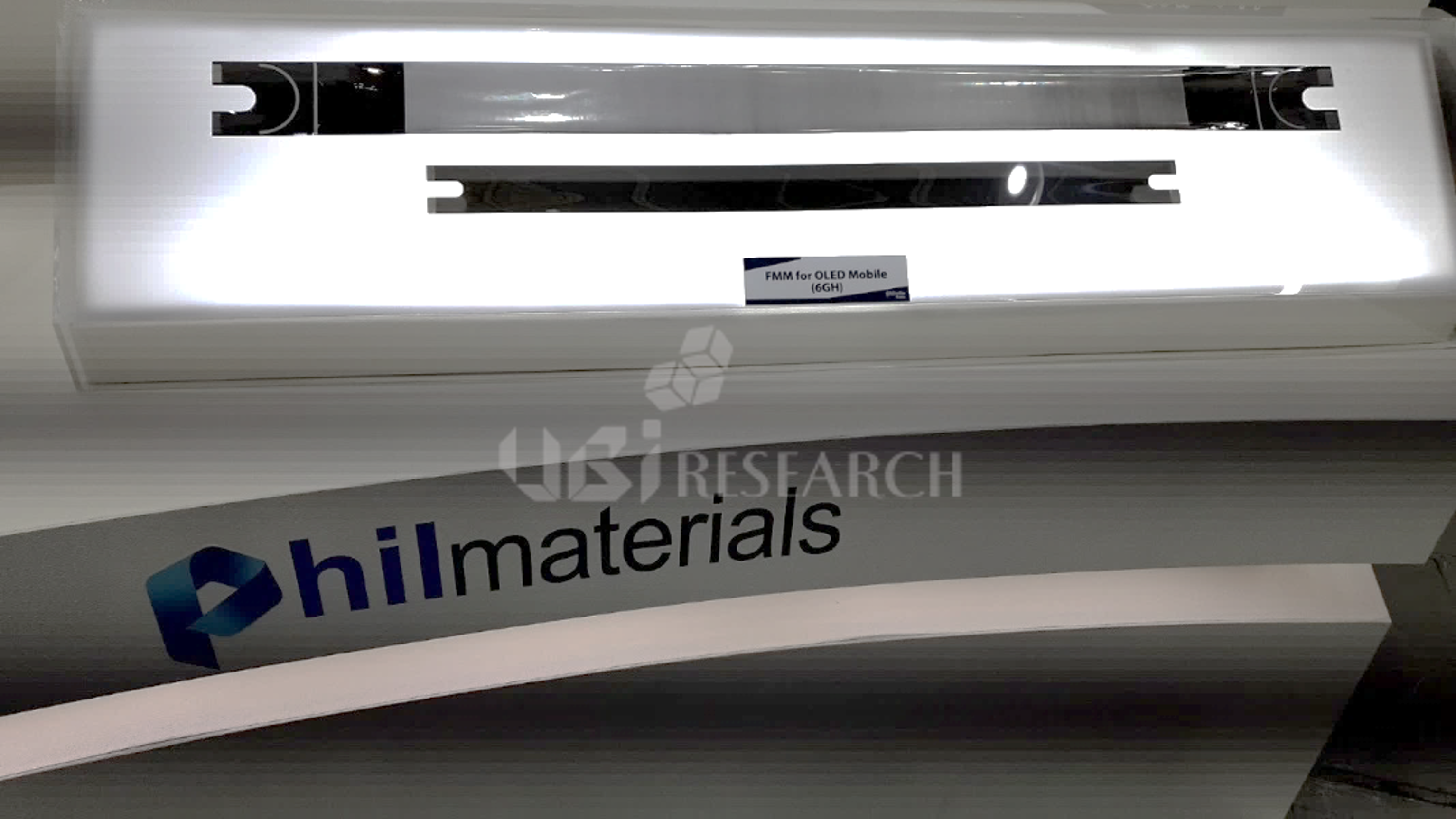
필머티리얼즈의(Philmaterials) FMM (OLED 모바일용 6GH)

필머티리얼즈의(Philmaterials) FMM (OLED 모바일용 6GH)

메탈 마스크에 쓰여지는 Invar는 OLED 제조에서 RGB를 증착용 FMM의 제작에 필요한 철-니켈 합금 소재이다. 필머티리얼즈에서는 Invar를 전주도금 공법을 이용하여 낮은 열팽창률과 얇은 두께를 가지므로 초고해상도 디스플레이 소재로 사용되고 있다. 압연방식의 FMM 대비 Pixel Shadow 개선이 가능하다. 6G half 크기의 OLED 모바일용 마스크와 IT용 mask도 전시 하였다.

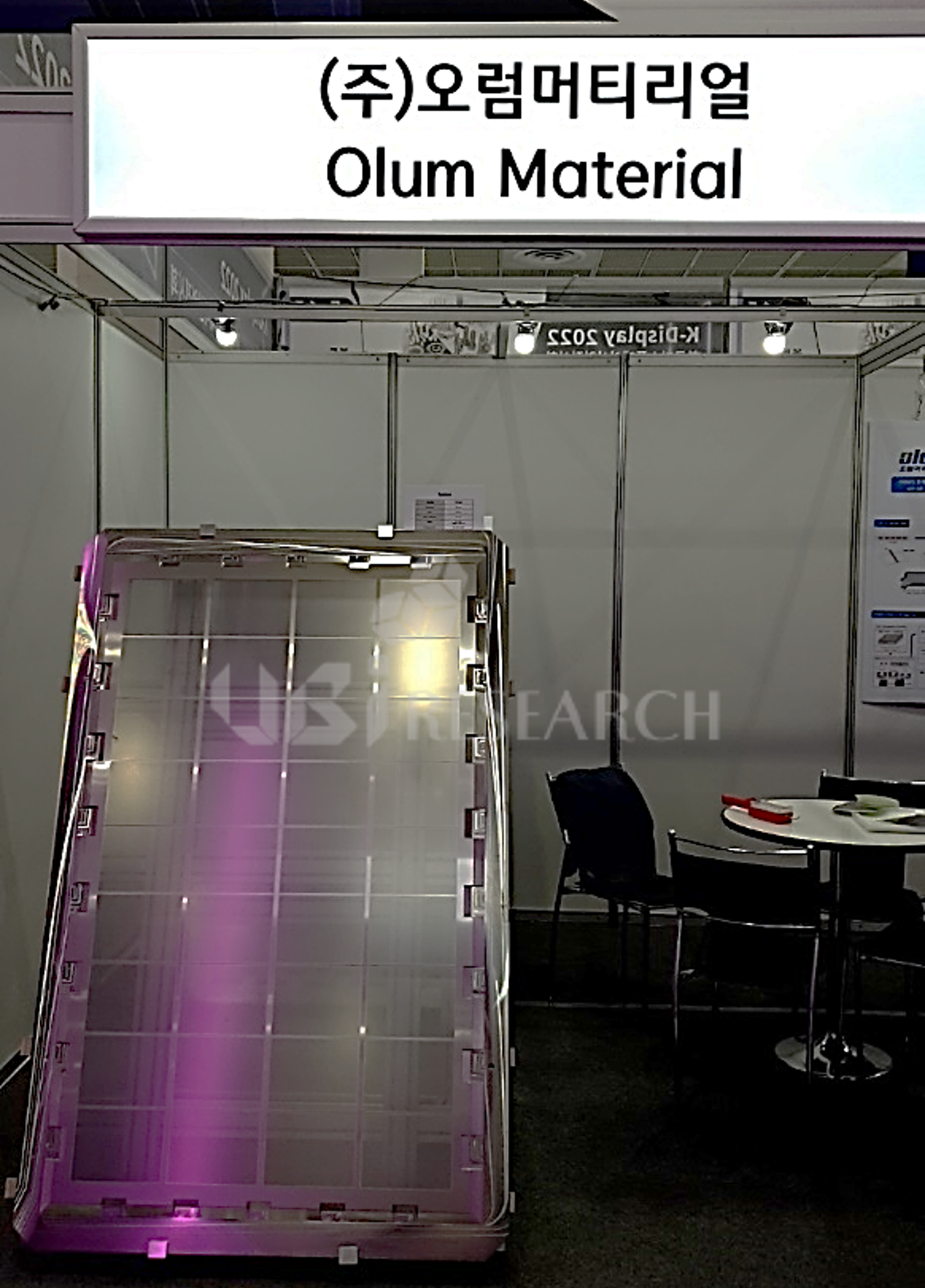
오럼머티리얼(Olum Mateial) FMM

오럼머티리얼(Olum Mateial) FMM

오럼머티리얼은 기존의 FMM 방식과는 달리 프레임에 개별 cell을 붙이는 방식을 이용했다. 대면적일 경우 처짐을 방지하는데 효과가 있으며 mask의 불량이 생길 경우 전체를 교체하지 않는 장점이 있다. 6G half 크기의 mask를 전시하였으며 국산화에 앞장서서 개발하고 있다.

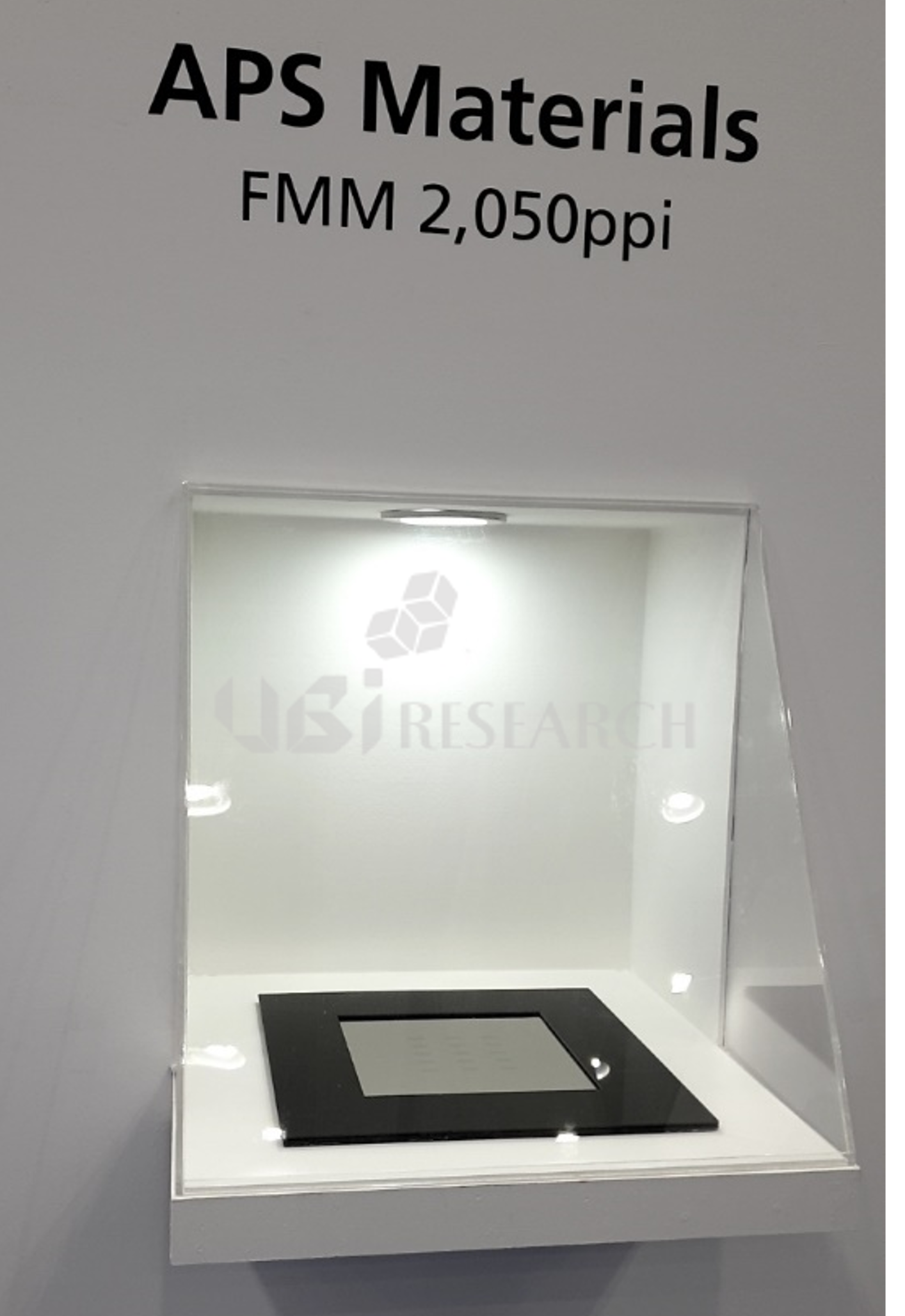
APS머티리얼즈(APS Materials) FMM(마이크로 OLED용)

APS머티리얼즈(APS Materials) FMM(마이크로 OLED용)

마이크로 OLED용 FMM은 더욱 미세한 홀을 요구하기 때문에 APS머티리얼즈는 고출력 레이저를 활용한 패터닝 레이저 기술을 도입하여 AR 및 VR용 디스플레이 분야에 사용하는 8인치 웨이퍼 기판에 패터닝 할 수 있는 2,050ppi FMM을 전시하였다.

▶2022 OLED 부품소재 보고서 Sample 보러가기 

[상반기 OLED 결산 세미나] 그래핀랩,도금 메탈 마스크로 ppi 한계 넘는다

그래핀 상용화 기술 기업인 GrapheneLab에서 그래핀을 이용한 800ppi 이상의 FMM 제조가 가능하다고 발표했다.
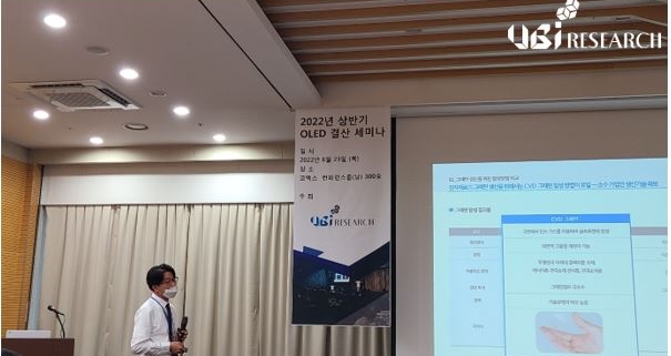
23일 서울 삼성동 코엑스에서 열린 ‘유비리서치 2022년 상반기 OLED 결산 세미나’에서 GrapheneLab의 권용덕 대표는 “2000년대 초반부터 시작된 FMM 기술은 초기에는 plating 방식에는 관심이 없었지만 최근에는 FMM 제조 기술 트렌드가 plating방식으로 변화하고 있다”고 말하며 “2013년도 이후에는 plating 방식의 FMM 제조 기술 관련 특허가 많이 출원되었으며, 고 해상도로 가기 위해서는 현재 사용되는 etching 방식보다 plating 방식을 적용하는 것이 용이하다”고 언급했다.


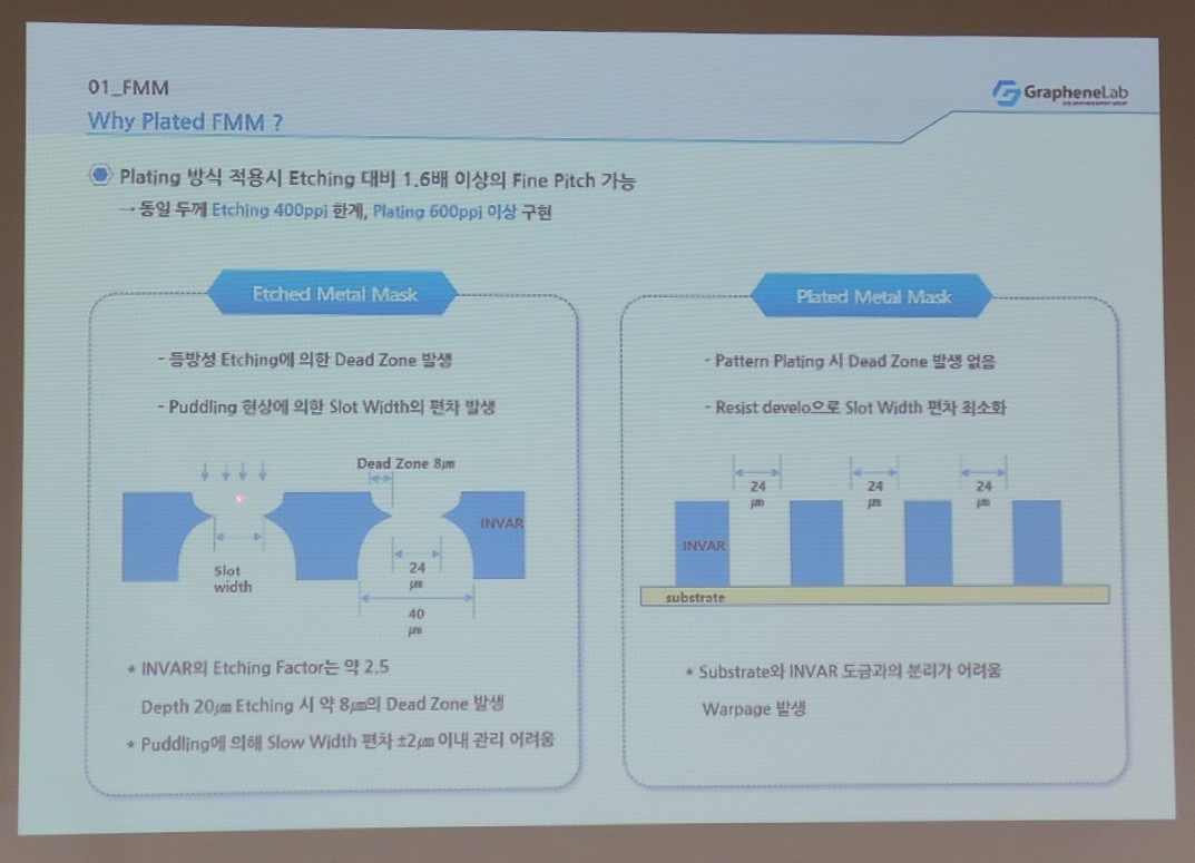
이어 권 대표는 “기존의 한계가 있던 etching 방식 FMM에서 벗어나 plating 방식의 FMM을 적용한 결과 동일한 두께에서 400ppi가 한계였던 etching 방식에 비해 plating 방식에서는 600ppi 이상을 구현했다”고 말하며 “Etched metal mask는 깊이 20um etching시 점처럼 뾰족해지는 INVAR 구조에 의해 8um길이의 dead zone이 발생되는 반면 plated metal mask의 pattern plating시에는 dead zone의 발생이 없다”고 발표했다.
끝으로 권 대표는 “MSAP electro forming 기술을 위해서 얇은 두께의 낮은 열팽창계수가 필요하다. Plated된 시료를 대상으로 TMA를 이용해 열팽창계수를 측정한 결과 3.1ppm까지 로 측정되었으며, 열처리를 하지 않은 상태에서는 2.5ppm까지 내려갔다”고 강조하며 발표를 마쳤다.

LGD·BOE 중소형 OLED 확대…삼성SDI, 미소 짓는 이유는?… 外

[디지털데일리=김도현 기자] 유기발광다이오드(OLED) 시장 확대로 관련 소재 업체가 웃는다. 노발레드를 자회사로 두고 있는 삼성SDI도 대상이다. 배터리 사업이 본격화한 가운데 OLED 분야까지 실적 개선에 힘을 보탤 전망이다. 30일 삼성SDI에 따르면 노발레드는 작년 매출액 1431억원, 당기순이익 518억원을 기록했다. 각각 전년대비 12.3%, 7.9% 상승했다.

[더벨=조영갑 기자] OLED 디스플레이용 메탈마스크 전문제조 업체인 풍원정밀은 ‘꿈의 은박지’라고 불리는 파인메탈마스크(FMM)의 양산 공급을 목전에 두고 있다. 고객사 향 공정 테스트가 막바지 단계에 접어든 것이다. 이 때문에 국내 업체 중 가장 먼저 일본 다이닛폰프린팅(DNP)이 장악하고 있는 중소형 FMM 시장에 균열을 일으킬 것으로 기대를 모으고 있다. 풍원정밀은 1996년 설립된 OLED(유기발광다이오드) 박막 금속 가공 전문기업이다. 비상장 기업으로 자본시장 내의 인지도는 높지 않지만, 20년이 넘는 ‘공력’과 탄탄한 글로벌 디스플레이 메이커 향 공급망으로 업계에선 이미 유명세를 얻고 있다. OMM(오픈메탈마스크) 시장을 과점하고 있는 주요 공급사다.

[아이뉴스24=서민지 기자] 삼성디스플레이가 모바일 플렉시블 유기발광다이오드(OLED) 시장에서 60%대 점유율을 유지하며 1위 자리를 굳건히 지켰다. LG디스플레이는 애플의 ‘아이폰12’ 효과로 2위로 올라섰다. 30일 디스플레이 전문 시장조사기관 스톤파트너스가 발표한 ‘1분기 모바일용 OLED 출하 동향 분석’ 보고서에 따르면 전 세계 모바일용 AMOLED 모듈의 총 출하량은 1억4천60만 장으로, 전년 대비 31.5% 성장할 것으로 전망된다.

[아시아경제=차민영 기자] 프리미엄 스마트폰 핵심 부품인 커버 윈도우 소재 시장에서 울트라씬글래스(UTG)와 투명 폴리이미드(PI)의 미래 전망이 극명하게 엇갈렸다. 폴더블폰이 각광받으면서 UTG 소재 수요는 늘었지만 투명 PI는 보급형 스마트폰 모델·태블릿PC·노트북향 부품으로 입지가 좁아지는 추세다. 30일 유비리서치의 보고서에 따르면, 2021년 현재 UTG와 투명 PI 시장 간 규모 차이는 1억4570만달러(약 1650억원) 수준이나, 2025년에는 6억5890만달러(약 7460억원)로 벌어질 전망이다. 시장점유율은 약 80대 20 수준을 꾸준히 유지할 전망이다.

[파이낸셜뉴스=박종원 기자] 세계 3위 스마트폰 제조사로 떠오른 중국 샤오미가 이달 고급형 스마트폰을 내놓으며 삼성이나 애플 등과 본격적으로 경쟁할 준비를 갖췄다. 업계 전문가들은 중국 화웨이가 미국의 제재로 휘청거리는 사이 샤오미가 빈틈을 노리고 있다고 분석했다.

29일(현지시간) 미 경제매체 CNBC에 따르면 샤오미는 이날 중국 시장에서 세계 시장을 겨냥한 최고급 스마트폰 ‘미11’을 출시했다. 해당 제품은 라이트 및 라이트 5G(5세대), 프로, 울트라까지 3종으로 출시됐다. 기격은 5999~6999위안(약 103만~120만원)이다. 해당 제품들이 언제쯤 중국 외에서 팔릴 지는 확인되지 않았다.

[디지털데일리=이안나 기자] 삼성전자가 포문을 연 접는(Foldable, 폴더블) 스마트폰 시장이 올해 본격적으로 성장할 전망이다. 화웨이·샤오미·오포 등 중국업체들이 순차적으로 폴더블폰을 선보이면서 기술력을 내세우고 있다. 삼성전자는 신기술을 대거 탑재한 갤럭시Z폴드3(가칭) 포함 최소 3종을 준비하며 선두 자리를 이어간다. 30일 관련 업계에 따르면 삼성전자는 7월 공개를 목표로 폴더블폰 신제품 준비에 박차를 가하고 있다. 기존 제품과 동일하게 들어가는 공통 재료들은 양산 준비를 끝내고 새롭게 들어가는 부품들도 테스트가 거의 완료돼가는 상황. 단 갤럭시Z폴드3에 신기술이 대거 적용되는 만큼 양산 가능 시점에 따라 공개 시기는 조정될 수 있다.

OLEDON, ‘초격차’ OLED 제조용 면소스 증착기술 공개

2018년 10월 24일부터 서울 코엑스에서 열리고 있는 IMID2018에서 OLED 증착장비 개발 벤처회사인 OLEDON이 ‘경쟁 국가들과의 초격차를 유지하기 위한’ OLED 제조 기술인 면소스 증착기술을 공개하여 이목을 집중시키고 있다.

OLEDON의 황창훈대표는 “한국이 현재의 OLED 생산국 1위를 앞으로도 유지하려면 창의적인 증착 기술개발 도전에 적극 투자하여야 한다”며, “미래의 중소형 및 대형 OLED 제조는 모두 면소스 증착기술이 사용될 것”이라 전망했다.

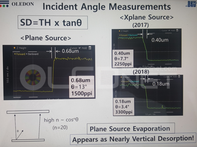
OLEDON이 세계최초로 개발 중인 곡면소스 FMM 증착기술은 2250ppi의 AMOLED 제조가 가능한 초고해상도 OLED 증착기술로서, 미세 패턴의 섀도우거리가 0.18um까지 가능하여 11K급 초고해상도의 AMOLED 패턴공정이 가능하다.

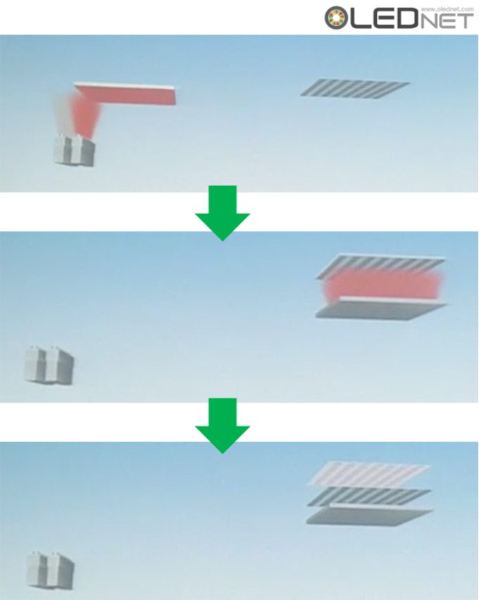
기존의 FMM 증착 패턴(좌)와 면소스 FMM 증착 패턴(우), Source: OLEDON

황 대표는 이러한 공정을 800ppi 섀도우 마스크로 확인한 결과, 면소스로 증착한 패턴의 발광면적이 기존의 증착 방법보다 1.7배 향상되었다고 발표하였다.

한편, OLEDON은 면소스 FMM증착기술의 원천특허를 보유하고 있으며 최근에는 대면적 OLED TV 제조용 수직형 면소스증착 특허를 출원하기도 하였다.

OLED TV 제조용 수직형 면소스 증착, Source: OLEDON


LCD Smartphone is 4K era, what about OLED Smartphone?

In the past MWC 2017, Sony unveiled the world’s first Smartphone with 4K LCD and it is scheduled to release the Xperia XZ2 Premium with 4K LCD on July 4. Attention is growing whether 4K resolution market is to be launched in earnest in smartphones.

<Xperia XZ2 Premium of Sony, Source: theverge.com>

TV market is already moving beyond the 4K to the 8K. Samsung Electronics and Sharp released new TVs with 8K resolution in the first half and Sony plans to release 8K TVs in the second half. LG Display also exhibited 88inch 8K OLED TV at CES 2018. As such, 8K TV is entering the premium TV market, and smart phones are expected to increase the number of products with 4K resolution in response to the higher resolution of TVs.

In the Smartphone, 4K has been implemented in LCD; however, in the case of OLED, QHD resolution is still dominant for the 4 consecutive years.

<Resolution change of Samsung Galaxy series, Source: UBI Research DB>

This is because there are many restrictions on the fine metal mask (FMM) technology that is being applied to OLED manufacturing. The thickness of FMM applied to the current production is about 20 ~ 30um. For 4K fabrication, the thickness should be as thin as 10um, but it is difficult for existing FMM manufacturing method.

As a result, FMM replacement technologies are being developed for high resolution implementation. Typical technologies under developing, include laser FMM patterning with laser, electroforming manufactured by electroplating method, a fine hybrid mask that is used to form a frame by electroplating on a film and pattern the film with a laser, and a surface source that realizes a high resolution by vertically setting the deposition incident angle.

Deposition technologies for high-resolution manufacturing at various exhibitions and conferences are being introduced. Depending on the availability for securing mass production, it is expected to see not only 4K OLED Smartphone, but also high-resolution AR and VR devices of RGB method.

LCD 스마트폰은 4K시대, OLED 스마트폰은?

지난 MWC 2017에서 소니가 세계 최초로 4K LCD를 탑재한 스마트폰을 공개한데 이어 오는 7월 4K LCD가 탑재된 Xperia XZ2 Premium을 출시할 예정으로 스마트폰에서도 4K 해상도 시장이 본격적으로 열릴 것으로 기대되고 있다.

<Sony의 Xperia XZ2 Premium, Source : theverge.com>

이미 TV시장에서는 4K를 넘어서 8K 시장으로 옮겨가고 있는 중이다. 삼성전자와 샤프는 상반기 8K 해상도의 TV 신제품을 공개하였으며, 소니도 8K TV를 하반기 출시 예정이다. LG Display에서도 88inch 8K OLED TV를 CES 2018에서 전시를 하였다. 이처럼 8K TV가 프리미엄 TV 시장에 진입을 하면서 스마트폰도 TV의 고해상도화에 대응하여 4K 해상도를 가진 제품 출시가 증가할 것으로 예상된다.

하지만 스마트폰에서 LCD는 4K를 구현했지만 아직 OLED는 4년째 QHD 해상도에 머물러있는 상황이다.

<삼성전자 갤럭시 시리즈의 해상도 변화, Source : UBI Research DB>

OLED제조에 적용되고 있는 FMM(fine metal mask) 기술에 제약이 많이 있기 때문이다. 현재 양산에 적용되고 있는 FMM의 두께는 약 20~30um 수준이며, 4K 제조를 위해서는 두께가 10um 수준으로 얇아져야 하지만 기존 FMM 제조방식으로는 어려움을 겪고 있는 상황이다.

이에 따라 고해상도 구현을 위한 FMM 대체기술들이 개발되고 있다. 대표적인 기술로는 레이져로 패터닝을 하는 laser FMM과 전주도금방식으로 제조하는 electroforming, 필름에 전주도금으로 프레임을 형성하고 레이져로 film을 패터닝하는 fine hybrid mask, 증착 입사각을 수직으로 하여 고해상도를 구현하는 면소스 등이 개발 중에 있다.


각종 전시회와 학회에서 고해상도 제조를 위한 증착기술들이 공개되고 있는 추세이며, 양산성 확보여부에 따라 앞으로 4K OLED 스마트폰, 더 나아가 RGB 방식의 고해상도 AR, VR 기기를 볼 수 있을 전망이다.

[SID 2018] OLEDON, presented about X-mixing plane source deposition technology for AMOLED efficiency enhancement.

In SID 2018, Hwang Chang-Hoon, CEO of OLEDON, announced a new plane source FMM deposition technology that can produce ultra-high resolution AMOLED of 2,250 ppi.

According to the announcement, the linear source currently applied to mass production has a problem of causing superimposition of fine adjacent patterns in a high resolution implementation due to a shadow distance of 3 μm. But Hwang said he succeeded in reducing the shadow distance of the patterns by 0.18 um using plane source, which is the smallest shadow distance ever introduced.

<Shadow effect comparison between current process and the process applied with the plane source, Source: OLEDON>

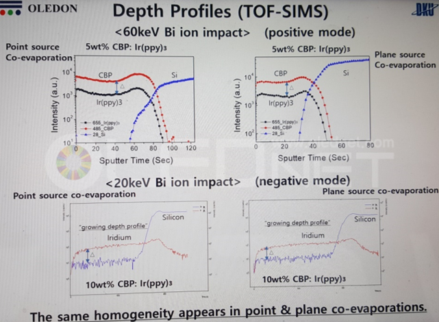
Hwang added that he developed ‘X-mixing’ technology in which the host and dopant thin films were separately deposited on the metal surface and then the host molecules and dopant molecules were automatically diffused through the plane evaporation to form the light emitting layer. Hwang commented, “It is not easy to control the composition of the dopant by using the linear source evaporation technology, which vaporizes the host material and the dopant material at the same time. However, since X-mixing technology can control the composition, it is possible to achieve a material utilization rate up to 4 times higher than the conventional method.”

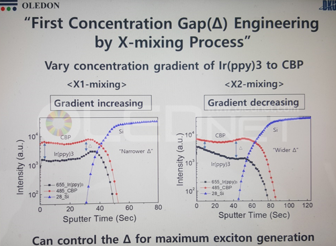
<SIMS data comparison between the emitting layer deposited by conventional method and the emitting layer deposited by the plane source, Source: OLEDON>

<Dopant gradient data of the emitting layer applied with X-mixing technology, Source: OLEDON>

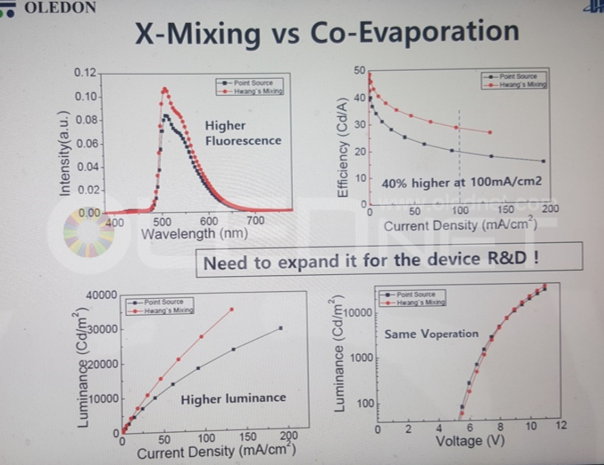
Hwang said, “In case of green OLED produced by X-mixing technology, 40% improvement in the emitting efficiency was verified, compared to the existing technology. OLEDON is currently under development of the optimized X- mixing development for forming exciton and the mask aligner with new concept sub-micron precision.

<Luminance data for green OLED produced by X-mixing technology and green OLED produced by the conventional method, Source: OLEDON>

Finally, Mr. Hwang mentioned that based on the development results, he plans to install a plane source FMM evaporator capable of manufacturing ultra-high resolution micro OLED devices in Dankook University.  (Reference: OLEDON homepage: www.oledon.co.kr)

[SID 2018] OLEDON, AMOLED 효율 향상용 X-mixing 면소스 증착 기술 발표

SID 2018에서 OLEDON의 황창훈 대표는 2,250ppi의 초고해상도 AMOLED를 제작 할 수 있는 새로운 면소스 FMM 증착기술을 발표했다.

발표에 따르면, 현재 양산에 적용 중인 리니어 소스는 3um의 섀도우 거리(shadow distance)로 인해 고해상도 구현 시 미세 인접 패턴들의 중첩을 발생시키기는 문제가 발생한다. 하지만 황대표는 면소스를 이용해 패턴들의 섀도우 거리를 0.18 um까지 줄이는데 성공하였다고 밝혔으며, 이는 현재까지 발표 된 섀도우 거리 중 가장 최소의 섀도우 거리라고 설명했다.

<기존 공정과 면소스를 이용한 공정의 섀도우현상(shadow effect) 비교, Source: OLEDON>

아울러 황대표는 호스트박막과 도판트박막을 따로 금속면에 증착 한 후 면증발을 통해 호스트 분자와 도판트 분자가 자동 확산되어 발광층이 형성되는 ‘X-mixing’기술을 개발하였다고 발표하였다. 황대표는 “기존 기술인 호스트 물질과 도판트 물질을 동시에 기화되는 리니어 소스 증착기술로는 도판트의 조성 제어가 쉽지 않으나, X-mixing 기술은 조성 제어가 자유자재로 가능하기 때문에 기존 대비 4배까지 향상 된 물질 사용률 달성이 가능하다”고 밝혔다.

<기존방식으로 증착 된 발광층과 면소스로 증착 된 발광층의 SIMS 데이터, Source: OLEDON>

<X-mixing 기술로 얻은 발광층의 dopant gradient 데이터, Source: OLEDON>

황대표는 “X-mixing 기술로 제작한 green OLED의 경우 기존 기술보다 40% 향상 된 발광효율을 확인하였다”고 언급하며 “OLEDON은 현재 소자의 발광효율향상을 목적으로 엑시톤형성의 최적화 된 X-mixing 개발과 신개념의 sub-micron 정밀도를 지닌 mask aligner를 개발 중”이라고 밝혔다.

<X-mixing 기술로 제작 된 green OLED와 기존 방식으로 제작 된 green OLED의 발광 데이터, Source: OLEDON>

마지막으로 황대표는 이번 개발결과를 토대로 초고해상도 마이크로 OLED 소자의 제조가 가능한 연구용 면소스 FMM 증착기를 단국대학교내에 설치할 계획이라고 언급했다. (참고:OLEDON사의 홈페이지 www.oledon.co.kr)

초고해상도를 구현할 수 있는 FMM, 국산화 앞당겨지나

Fine metal mask(이하 FMM)은 화소와 RGB 유기물을 증착하는 역할을 하기 때문에 FMM은 OLED의 해상도와 수율을 결정짓는 요소로서 작용되나, 현재 FMM은 증착 공정시 열팽창이 일어나거나 무게에 의한 섀도우 현상이 발생하는 한계에 봉착해 있다.

또한, FMM 전량은 일본 히다치(Hitachi)금속이 생산한 압연 invar를 일본 다이니폰프린팅(DNP)에서 에칭 공정을 통해 만든 완제품 형태로 비싼 가격에 수입하고 있다.

이로 인해 국내외 관련 업계는 laser가공 등 다양한 방식으로 FMM 개발에 총력을 기울이고 있는 상황이나 아직까지 R&D 단계에 머물고 있는 실정이다.

이런 상황에서 지난 9일 순천대학교 신소재공학과 박용범 교수 연구팀은 전주도금 인바 제조기술을 개발에 성공했다고 밝혔다. 이는 전기도금을 활용하면서 음극에 부착된 금속을 박리한 후 형상이 있는 부품으로 만드는 기술이다.

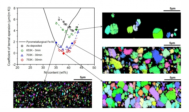
<전주도금인바의 열팽창곡선과 미세조직, 출처: 순천대>

해당 기술을 통해 invar는 판재로도 생산할 수 있고, 패턴 된 음극의 형상을 그대로 복제할 수 있다. 또한, FMM의 두께를 지금보다 절반 정도 얇은 7 um 수준까지 구현할 수 있어 초고화질을 구현할 수 있다고 연구팀은 설명했다.

박 교수는 “전주도금 인바에 대한 일본의 연구 수준이 우리 연구팀 턱 밑까지 쫓아왔고, 중국은 대규모 자본을 앞세워 개발에 뛰어들었다.”며, “우리나라 기업들이 국제경쟁력을 선점하기 위해서는 학계가 적극 지원할 필요가 있다고 판단했다.”고 말했다.

이에 따라”지난 20년 가까이 연구해 구축한 모든 데이터베이스를 논문을 통해 공개하기로 결심했다.”고 덧붙여, 그간 전량 수입에 의존하던 FMM을 국산화 할 수 있을지 귀추가 주목된다.

Is accelerating the localization for FMM, which can realize ultra-high resolution?

Since Fine Metal Mask (FMM) plays a role of depositing pixel and RGB organic materials, FMM is a factor that determines the resolution and yield of OLED. However, FMM is currently confronted with some limitations that thermal expansion occurs during the deposition process or shadow effects arise due to its weight.

In addition, the total amount of FMM is imported at high prices in the form of finished products which are made by Japanese Dainippon Printing (DNP)’ etching process with the rolled invar produced by Hitachi Metals.

Under the circumstances, domestic and overseas related industries are concentrating on developing FMM in various ways such as laser processing, but they are still in R & D stage.

The research team of Professor Park Yong-Bum of New Material Engineering Department of Sunchon University announced on 9th May that it succeeded in developing the technology of electroforming invar manufacturing technology. This is a technique for separating the metal attached to the cathode while utilizing the electroplating, and making FMM.

<Thermal expansion curves and microstructure of electroforming invar, source: Suncheon University>

According to the research team, invar can be produced as a sheet material, and the shape of the patterned cathode can be copied as it is, through this technology. In addition, the thickness of FMM can be reduced to about 7μm, about half the thickness of the current FMM, which might be helpful to realize super high image quality.

Professor Park said, “The level of Japanese research on the electroforming invar has been pursued to the bottom of our research team, and China has entered into development with a large amount of capital.” In order for Korean companies to gain international competitiveness, I thought the academic circles needed to support it actively. Consequently, I have decided to publish all the databases that have been built and researched for nearly 20 years through papers.”

Attention is focused whether it is to be successful in localizing FMM, the total amount of which has been imported.

초고화질 해상도(UHD)의 OLED 스마트폰 시대 열릴까

최근 스마트폰 기기를 통한 VR 컨텐츠 체험이 증가하는 추세로 인해 고해상도 스마트폰이 요구되고 있으나, 2014년 Galaxy Note4에 최초로 QHD OLED가 적용된 이후 3년 동안 OLED 스마트폰의 해상도는 여전히 QHD급에 머물고 있다.

OLED 스마트폰의 해상도를 결정하는 핵심은 발광층의 증착 공정이다. 현재 적용 되고 있는 상향식 증착 방식은 기판과 FMM(fine metal mask)를 수평으로 하여 증착 장비 상부에 배치한 뒤 하부의 리니어 소스에서 유기물을 증발시켜 RGB 발광층을 형성하는 방식이다.

UHD급 이상의 고해상도 OLED를 제조하기 위해서는 15um 두께 이하의 얇은 FMM이 필요하나 FMM이 얇아질수록 patterning, 인장, 용접등의 기술적인 이슈가 발생하여 양산적용이 어렵다.

이러한 문제들을 극복하기 위해 수직형 증착과 면소스 증착, 다양한 metal mask patterning 기술들이 개발되고 있다.

기판과 FMM를 수직으로 배치하는 수직형 증착기는 일본의 Hitachi에서 최초로 개발하였으며,  Canon tokki도 Finetech Japan 2013에서 6세대 수직 증착 방식의 장비를 공개한바 있으나 현재 양산에 적용되고 있진 않다.


<Finetech Japan 2013에서 공개 된 Canon tokki의 Gen6 vertical type evaporator>

하지만 최근 전자신문에 따르면 Applied Materials에서 6세대 flexible OLED용 수직 증착 방식의 증착 장비를 개발했다고 밝혔으며, 일본의 Japan Display에서 test 중이라고 언급한바 있다.

리니어소스가 아닌 면소스를 이용한 증착 방식도 검토되고 있다. 면소스 증착 방식은 유기물을 금속면에 1차로 증착하여 면소스를 만든 후, 이를 재증발시켜 기판에 유기물 박막을 형성하는 원리로써 지난 iMiD 2017에서 OLEDON의 황창훈 대표는 면소스 증착 방식을 통해 2250 ppi의 고해상도 OLED 구현이 가능하다고 언급하였다.

Metal Mask patterning 기술로는 전주도금(electro forming)과 laser patterning 기술이 주로 거론되고 있다. 전주도금 방식은 Wave Electornics와 TGO Technology, Athene등의 업체에서 개발하고 있으며, laser patterning 기술은 AP Systems에서 개발중에 있다.

이처럼 다양한 관점에서 진행되고 있는 고해상도 OLED 구현을 위한 개발이 현재의 문제를 극복하고 OLED 스마트폰의 UHD 해상도 구현에 기여할 수 있을지 많은 관심이 집중되고 있다.

<OLEDON사가 개발한 면소스 증착 기술 원리>

Is there possibility of High resolution(UHD) OLED Smart-phone generation?

Recently VR contents experience through smart-phone device has been increased, therefore high resolution of smart phone is becoming necessary. However, OLED smart-phone resolution still remains at QHD level for 3 years since QHD OLED is applied to Galaxy Note 4 for the first time in 2014.

The core point that decides resolution of OLED smart-phone is evaporation process for emission layer. Bottom-up type evaporation method, which is applied to the recent devices is that substrate and FMM (fine metal mask) are horizontally arranged on the upper side of evaporator and vaporize the organic material from the lower linear source in order to form RGB layer.

Thin FMM measures less than 15um thick is necessary for making high resolution OLED like UHD level, however, as FMM gets thinner, it would be difficult to make mass production because technical problems will be occurred such as patterning, sealing and welding.

In order to solve these problems, various metal mask patterning technologies are being developed such as vertical type evaporation and plane source evaporation.

Vertical type evaporator that arranges board and FMM vertical is developed by Hitachi of Japan for the first time. And Canon Tokki exhibited Gen6 vertical type evaporator at Finetech Japan 2013, however it is not being used for mass production at the moment.

<Canon Tokki’s Gen6 vertical type evaporator which is exhibited at Finetech Japan 2013>


According to the recent ETNEWS, Applied Materials developed Gen6 flexible OLED vertical type evaporator and it is being tested in Japan Display.

Plane source evaporator is being tested but also the linear source type. Plane source evaporator method is that an organic material is first evaporated on the metal surface to produce plane source, then re-evaporated in order to form an organic thin film on the substrate.

In the past iMiD 2017, representative of OLEDON, Chang Hoon Hwang mentioned that 2250 ppi resolution OLED can be implemented through plane source evaporator.

For metal mask patterning technology, electro forming and laser patterning technology is highlighted. Electro forming method is developed by Wave Electronics, TGO Technology, Athene and so on. Laser patterning technology is being developed by AP Systems.

As such, development for high resolution OLED is receiving great attention whether it can solve the current problems and contribute to UHD resolution implementation for OLED smart-phone.

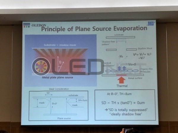
<Principle of plane source evaporation developed by OLEDON>

[iMiD 2017] AP Systems, USPL을 통해 FMM의 해답을 찾다

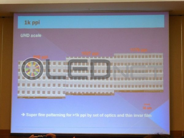
28일 부산 BEXCO에서 개최된 iMiD 2017에서 AP Systems는 USPL(ultra-short pulse laser)로 1000ppi FMM개발에 성공했다고 발표하였다.

FMM은 화소와 RGB 유기물을 증착하는 역할을 하기 때문에 FMM은 OLED의 해상도와 수율을 결정짓는 요소로서 작용된다. 현재 FMM은 주로 전주(etching) 방식으로 제작되고 있다. 이 방식은 미세 패턴의 정밀도와 두께, 무게에 의한 섀도우 현상이 발생하는 문제가 있어, 이를 해결하기 위해 laser 가공, 전해주조(electro-forming)등 다양한 FMM 제조 공정이 개발되고 있다.

이 중 laser 가공 방식은 laser 조사 시 발생하는 열(thermal effect)로 인해 pin-hole 주변에 burr가 형성되는 이슈가 있다. 이러한 burr는 FMM의 섀도우 구간을 증가, RGB 유기물 증착 시 패턴이 겹치는 현상을 야기시킴으로써 OLED의 해상도를 저하시킨다.

AP Systems는 이러한 점을 착안해 burr 현상이 없고, 나아가 taper angle을 제어하는 burr-free laser process을 개발하였다.

Burr-free laser process는 단방향 펄스를 일정 횟수로 나누어 짧게 조사하는 방식으로 연속적으로 laser를 조사하지 않기 때문에 축적되는 열 에너지가 최소화 되어 burr 형성을 막는다. 또한, laser의 energy를 제어함으로써 energy 축적하여 taper를 형성하는 방식이다.

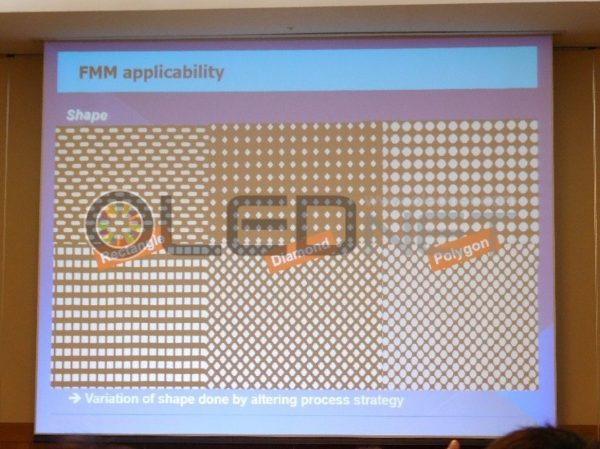
AP Systems는 이 방법을 통해 ‘1170ppi의 FMM 뿐만 아니라 미세 pin-hole의 모양이 사각형 또는 다이아몬드, 다각형 등 다양한 형태를 갖는 FMM도 제작하였다’며 ‘USPL 방식이 적용된 대면적 FMM 제조 장비도 개발하였다’고 설명하였다.

또한, AP Systems는 FMM 제조 장비에 대해 ‘multi-beam과 USPL이 장착되어 있어 생산성을 향상시킬 수 있으며, UHD를 구현할 수 있다’고 덧붙였다.

14년 Galaxy Note4 출시 이후부터 아직까지 OLED의 해상도는 QHD 급에 머물고 있다. 고해상도(UHD급 이상)를 가지는 OLED를 제조하기 위해서는 FMM이 기술적으로 직면하고 있는 다양한 문제를 해결해야 되는 실정이다. 이에 따라 AP Systems의 USPL 기술이 향후 OLED 시장에 어떠한 영향을 미칠지 앞으로의 귀추가 주목된다.

<AP Systems가 제작한 1000ppi FMM>


<다양한 형태의 FMM>

[iMiD 2017] AP Systems, Find FMM answers through USPL

At iMiD 2017 in BEXCO, Busan on 28th, AP Systems announced that it succeeded in developing 1000ppi FMM with USPL (ultra-short pulse laser).

Since FMM plays a role of depositing pixels and RGB organic materials, FMM serves as a factor that determines resolution and yield of OLED. At present, FMM is mainly manufactured by etching method. This method has a problem that a shadow phenomenon due to the precision, thickness, and weight of the fine pattern occurs, in order to solve this problem, various FMM manufacturing processes such as laser processing and electro-forming have been developed.

Among these, laser processing method has an issue of forming burrs around pin-holes due to the thermal effect caused by laser irradiation. These burrs increase the shadow interval of the FMM, which causes overlapping of patterns during RGB organic deposition, thereby degrading the resolution of the OLED.

AP Systems has developed a burr-free laser process that does not have burr phenomenon and further controls the taper angle.

The Burr-free laser process is a short-time irradiation of unidirectional pulses at a constant number of times, since the laser is not continuously irradiated, it minimizes accumulated heat energy and prevents burr formation. In addition, by controlling energy of the laser, it accumulates energy and forms taper.

In this way, AP Systems explained ‘they produced FMM with various shapes of fine pin-holes such as square, diamond, and polygonal shapes, as well as 1170ppi FMM’, and ‘’We also developed large-area FMM manufacturing equipment with USPL method’.

AP Systems also added ‘multi-beam and USPL is equipped for FMM manufacturing equipment so that it can improve productivity and realize UHD’.

Since the launch of the Galaxy Note4 in 2014, the OLED resolution has remained at the QHD level yet. In order to manufacture an OLED having a high resolution (UHD level or higher), it is necessary to solve various technical problems faced by FMM. Accordingly, it is noteworthy how USPL technology of AP Systems will affect the future OLED market.

<1000ppi FMM produced by AP Systems>


<various type of FMM produced by AP Systems>


Sunic System’s Successful Demonstration of 1.1um Shadow Distance, High resolution up to 1500 ppi

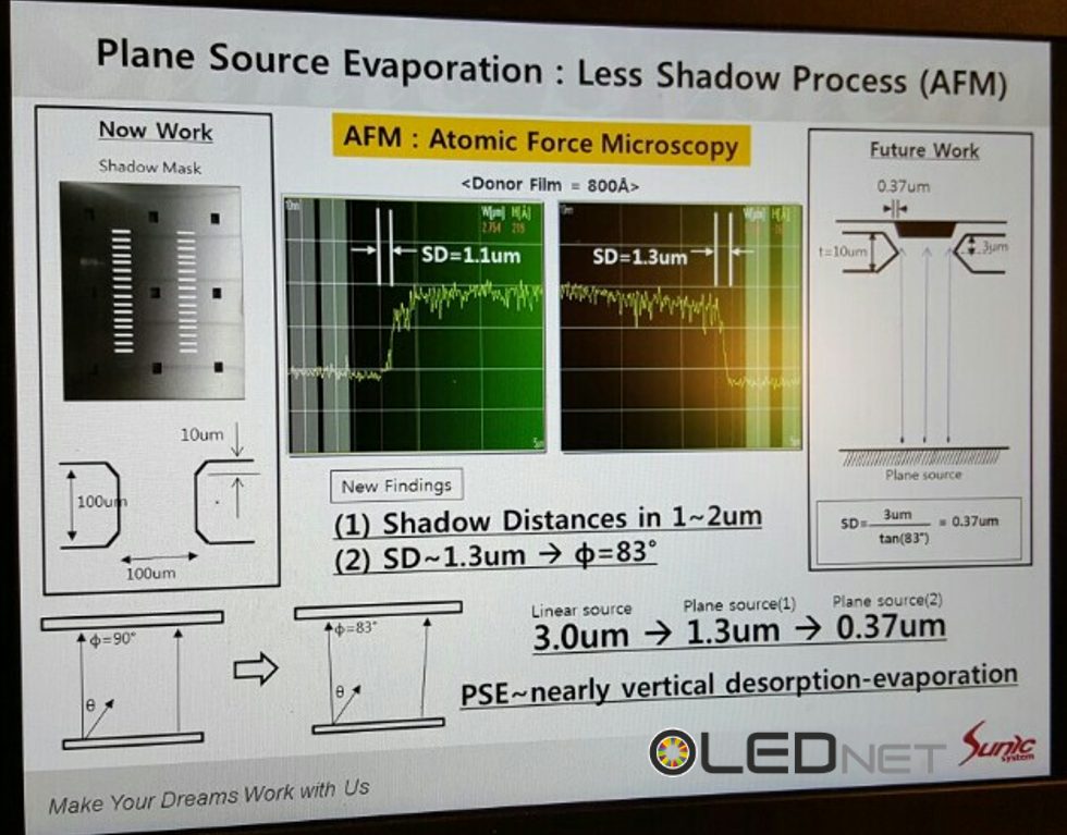
Sunic System announced at 2016 IMID Business Forum that it succeeded in implementing 1.1um shadow distance by using plane source evaporation and 100um shadow mask. 1.1um shadow distance is able to manufacture 1000ppi~1500ppi high resolution.

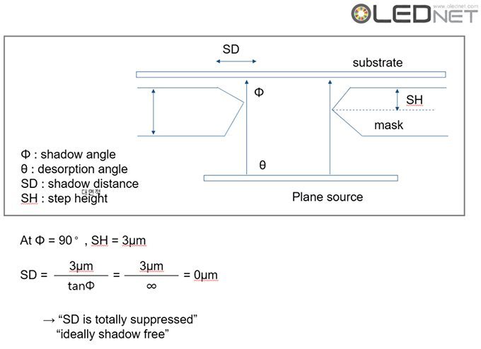
Plane source evaporation is a technology to evaporate OLED light-emitting material on metal plate, invert it, apply heat to the metal plate, and vertically evaporate OLED light-emitting material. When the shadow angle(Ф) of OLED light-emitting material evaporation is 90 degrees, the value of SD(Shadow distance, step height / tanФ) is zero (0) theoretically. So, it is possible to design thick and high resolution FMM, which means high-resolution AMOLED panel can be manufactured. This principle was announced for the first time at IMID 2016 Business Forum, attracting big attention.

Sunic System Dr. Hwang Chang-hoon said “If we lower step height up to 3um by reducing the thickness of shadow mask based on this result, 0.37um shadow distance would be possible, which means we can manufacture maximum 2250ppi(11K) high resolution AMOLED panel. Accordingly, we will put spurs to development of 0.37 shadow distance”.

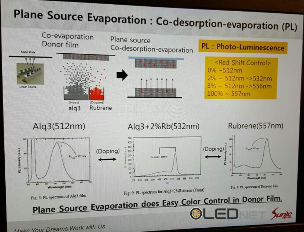
Also, he announced that co-evaporation of host and dopant that had been thought to be impossible in plane source has been resolved using flashing evaporation. He also proved that if donor film goes through flashing evaporation after co-evaporation of host and dopant, host and dopant can co-evaporate, and color control becomes easier by controlling dopant ratio to manufacture donor film.

1611021

<Result of Color Control after applying Flashing Evaporation>

1611022

<Result of 1.1um Shadow Distance>

선익시스템 1.1um shadow distance 데모 성공, 1500 ppi까지 구현 가능

선익시스템은 2016 IMID Business forum에서 plane source evaporation과 100um두께의 shadow mask로 1.1um의 shadow distance 구현에 성공했다고 발표했다. 1.1um의 shadow distance는 약 1000ppi~1500ppi의 고해상도 제작이 가능한 수치이다.

Plane source evaporation은 metal plate에 OLED 발광재료를 증착하고 뒤집은 후 metal plate에 열을 가함으로써 OLED 발광재료를 수직으로 증착시키는 기술이다. OLED 발광재료가 증착되는 shadow angle(Ф)이 90도가 되면 이론적으로 SD(Shadow distance, step hight / tanФ) 값이 0이 되기 때문에 FMM의 두께를 얇고 고해상도로 설계할 수 있어 고해상도 AMOLED panel 제조가 가능해 진다는 원리로서 지난 IMID 2016 학회에서 처음 발표되어 큰 관심을 끌었었다.

선익시스템의 황창훈 박사는 “이번 결과를 바탕으로 shadow mask 두께를 감소시켜 step height를 3um까지 감소시킨다면 0.37um의 shadow distance를 구현 가능하게 되고 이는 최대 2250ppi(11K)의 고해상도 AMOLED panel 제조가 가능해질 것” 이라며 0.37 shadow distance 구현을 위한 개발에 박차를 가할 것이라고 발표했다.

또한 이번 발표에서는 plane source에서는 불가능 할 것으로 예상됐던 host와 dopant의 co-evaporation을 급속가열(flashing evaporation)을 적용하여 해결 했다고 밝혔다. Donor film에 host와 dopant를 동시 증착한 후 donor film을 flashing evaporation을 하게 되면 host와 dopant를 동시에 증발시킬 수 있으며, donor film을 제작할 때 dopant ratio를 control 함으로써 color control을 쉽게 할 수 있음을 증명하였다.

1611021

<Flasing evaporation을 적용한 color control 결과>


1611022

<1.1um의 shadow distance를 구현한 결과>

A fabrication of large area OLED TV gets possible by FMM process. DAWONSIS, develops downward deposition method by joule heating.

It is expected that large area OLED panel pixel formation technology, which is possible only using solution based and SMS(Small mask scanning) so far, gets possible using FMM process.

DAWONSIS developed the technology downward deposition method by joule heating, to make mass production of large area display panel possible and to enhance efficiency of material usage more than two times.

Joule heating deposition is the technology that if one induces voltage in conductive film, due to resistance, it can increase surface temperature rapidly only with low energy, so evaporate organic materials films formed on conductive film rapidly only with low energy.

DAWONSIS evaporation technology key concept is followed by:

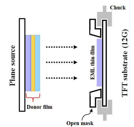
One forms organic material films on source substrates, and deposits the organic material films on panel positioned at down side whole at a time by using Joule heating.
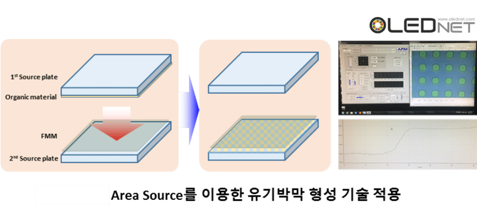
<Application of organic thin film formation technology>


According to DAWONSIS, it is said that

“Compared to point source or linear source, used in conventional deposition process, Joule heating deposition process is very fast deposition rate, more than 100 A/s, due to the use of area source. The efficiency of material usage is about 70~80%, more than two times efficient than conventional method, also downward deposition is applicable to large area FMM process, verification experiment results show that shadow effect dimension is 4um, which enables high resolution process. Therefore JIES evaporation equipment can be an innovative solution to fabricate large area OLED panel. ”
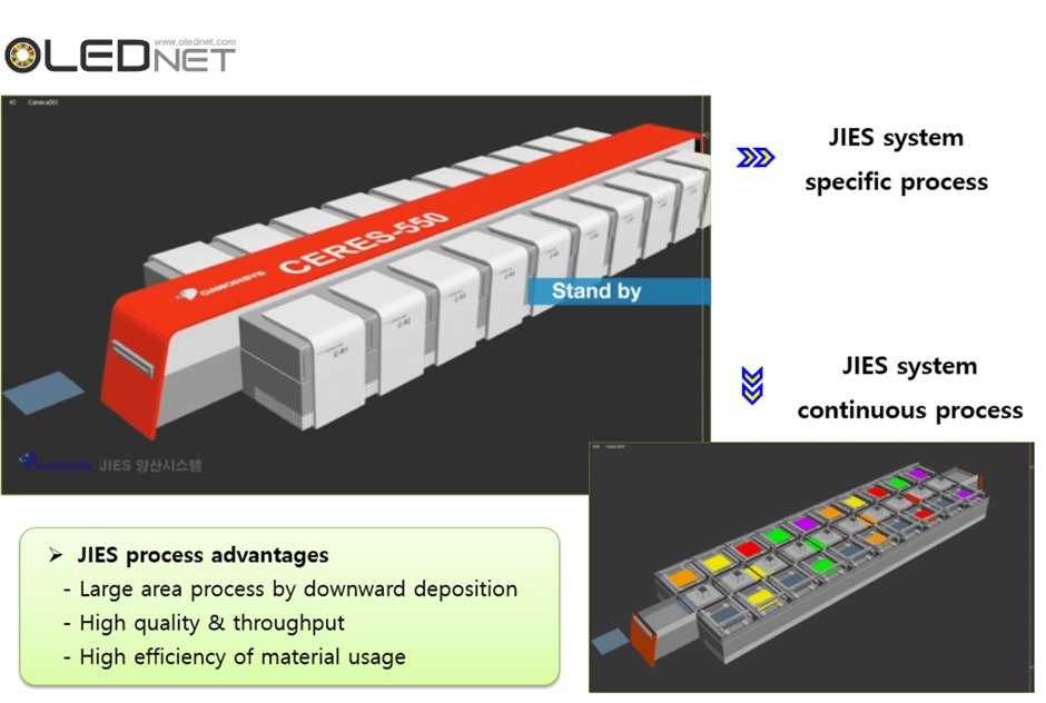
160912_2

In conventional OLED TV, due to FMM’s deflection, it has had a problem to fabricate it as RGB method. So OLED TV panel on production line, adopts white OLED + color filter method using open mask

In order to make OLED TV by using RGB method, solution process can be also strong candidate.

But lack of efficiency of soluble luminous material and its life time, it cannot be applicable to mass production.

If one adopts the deposition technology that DAWONSIS developed, real RGB structure can be realized in OLED TV panel by using FMM process, since it uses conventional deposition materials as it is, efficiency and life time can be guaranteed. We expect that DAWONSIS’s new deposition technology can make an impact on large area OLED panel fabrication technology.
대면적 OLED TV, FMM으로도 가능해진다. 다원시스, 주울 가열 하향식 증착 기술 개발

용액공정과 SMS(Small mask scanning)방식으로만 접근되었던 RGB 방식의 대면적 OLED panel용 화소형성 기술이 FMM으로도 가능해 질 것으로 기대된다.


다원시스는 대면적 디스플레이 패널 양산에 적용이 용이하고 재료사용효율을 기존 보다 2배 이상 향상시킨 주울 가열 증착 공정 방식의 하향식 증착 기술을 개발하였다.


주울 가열 증착 이란 도전성 박막에 전압을 가하면 저항으로 인하여 짧은 시간 안에 적은 에너지로 표면 온도만 빠르게 높여 도전성 박막 위에 형성된 organic material 막을 적은 에너지로 빠르게 증발 시킬 수 있는 기술이다.


다원시스에서 개발한 증착 기술 컨셉은 다음과 같다. 소스기판 위에 organic materials 박막을 형성하고 주울 가열을 사용하여 소스기판 표면의 organic materials을 전부 한번에 하부에 위치한 panel로 증착 시키는 방식이다.

160912_1

다원시스 관계자에 따르면 “기존 증착 공정에서 사용하는 point source 나 Linear source에 비해 주울 가열 증착 공정은 Area source를 이용하기 때문에 증착 속도가 약 100 A/s 이상으로 굉장히 빠르다. 또한 재료사용 효율이 70~80%로 기존 증착공정대비 2배 이상 향상되며 하향식 증착으로 대면적에 FMM 방식이 적용 가능하고, 검증 실험 결과 shadow effect dimension이 4 μm 로서 고해상도 구현이 가능하다. 따라서 JIES 증착 장비는 대면적 OLED의 새로운 solution이 될 수 있을 것” 이라고 밝혔다.

160912_2

기존의 대면적 OLED TV는 FMM의 처짐 현상으로 인하여 RGB 방식으로의 제조에 어려움을 겪고 있었다. 따라서 현재 양산중인 OLED TV용 panel은 open mask를 적용한 white OLED + color filter 방식을 적용하고 있다.

또한 대면적 OLED TV를 RGB 방식으로 제조하기 위해 solution process도 적극적으로 개발 중이지만 soluble 발광재료의 효율과 수명 이슈로 아직까지 양산에 적용되고 있지 못하는 상황이다.

하지만 다원시스에서 개발한 증착 기술을 적용하면 FMM을 적용한 진정한 RGB 구조의 OLED TV용 panel 제조가 가능해지며, 기존 사용되고 있는 증착 재료를 그대로 적용 가능하기 때문에 효율과 수명도 확보할 수 있다.

이번 다원시스의 새로운 증착 기술이 앞으로의 대면적 OLED panel 제조 기술에 어떤 영향을 미칠지 기대된다.

선익시스템, plane source기술로 고해상도 11K AMOLED panel 해법 제시

제주도 ICC 컨벤션 센터에서 열린 IMID2016에서 선익시스템의 11K(2250 ppi) AMOLED 제조를 위한 솔루션이 화제가 되고 있다.

올해 초 개최된 제 2회 OLED Korea Conference에서 삼성디스플레이의 황인선 수석연구원은 “VR에서는 고해상도가 핵심이며 약 2000ppi 정도 되어야 VR 디바이스에서 현장감을 잘 느낄 수 있을 것’이라고 발표하며, VR에서는 디스플레이를 접하는 거리가 가깝기 때문에 해상도가 떨어진다는 점을 해결해야할 과제로 꼽았다.

하지만 현재 mobile 기기용 AMOLED panel의 최고 해상도는 삼성디스플레이가 SID2016에서 공개한 806 ppi가 최고 해상도이다.

현재 AMOLED panel 양산에 적용중인 기술은 선형소스에서 OLED 발광재료를 열로 증발시키고 증발된 OLED 발광재료가 FMM(fine metal mask)를 통과하여 기판에 증착되는 원리이다.

하지만 OLED 발광재료의 증착과정에서 증착 소스와 FMM 사이의 거리와 FMM의 두께, FMM과 기판 사이의 거리로 인하여 OLED 발광재료가 FMM을 통과할 시 입사각(θ)이 생기게 되며, 입사각으로 인하여 SD(shadow distance)가 발생하게 된다. SD이슈로 인해 FMM을 설계시 SD를 최소화 하는 mask의 두께와 step hight를 결정해야 하며 이는 고해상도 FMM 제조를 어렵게 하는 주요 원인이다.

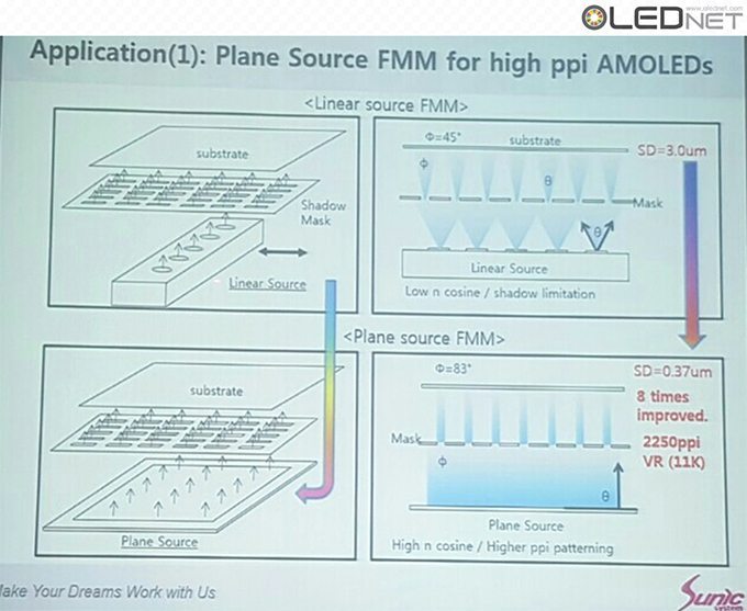
Shadow distance 원리, 선익시스템 IMID2016

Plane Source Process, 선익시스템 IMID2016

Plane source의 적용 application, 선익시스템 IMID2016

Plane source의 적용 application, 선익시스템 IMID2016

선익시스템에서는 이러한 문제점을 해결하기 위해 linear source가 아닌 plane source를 제안하였으며, 이는 고해상도 AMOLED panel의 핵심 기술이 될 것으로 발표했다. Plane source기술은 metal plate에 OLED 발광재료를 증착하고 뒤집은 후 metal plate에 열을 가함으로써 OLED 발광재료를 수직으로 증착시키는 기술이다. OLED 발광재료 shadow angle(Ф)이 90도가 되면 이론적으로 SD(Shadow distance, step hight / tanФ) 값이 0이 되기 때문에 FMM의 두께를 얇고 고해상도로 설계할 수 있어 고해상도 AMOLED panel 제조가 가능해 진다.

 선익시스템의 황창훈 박사는 “plane source를 이용하면 SD값을 기존대비 약 8배 까지 줄일 수 있어 VR용 11K(2250 ppi) AMOLED panel 구현이 가능해지며, 대면적 SMS 증착기술에서도 8K(200 ppi) RGB OLED TV용 panel 제조가 가능해진다.”라고 설명 하였다.

특히 plane source를 적용한 SMS 증착기술이 대면적에 적용이 가능해지면, 대면적 OLED panel 제조 기술에도 큰 파장을 일으킬 수 있을 것으로 예상된다.

현재까지는 RGB 방식으로 대면적 OLED panel 제조를 위한 기술로는 inkjet printing을 적용한 solution process이 중점적으로 개발되고 있지만, soluble OLED 발광재료의 성능이 기존 증착용 OLED 발광재료보다 낮은 이슈가 있었다. 하지만 plane source 기술이 성공적으로 개발, 적용가능해 진다면, 증착용 OLED 발광재료를 그대로 사용할 수 있기 때문에 solution process OLED를 대체하는 대면적 OLED Panel제조기술이 될 수 있을 것으로 기대된다.

한편 선익시스템은 LG Display에 국내 장비업체 최초로 Gen6 증착장비를 납품하였으며, 2018년부터 본격적인 양산이 가능할 것으로 예상된다.

Visionox, 604PPI의 고해상도 디스플레이 기술을 개발하다.

11월 12일 Visionox에 따르면 최근 FMM(Fine Metal Mask)을 사용한 증착기술을 통해 604PPI(약 4.85inch)의 고해상도 full color OLED 패널을 개발했다고 밝혔다.

Visionox Z-Type(Source : OLED-info)

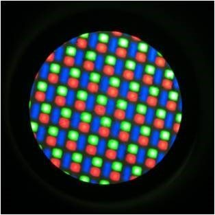
Visionox는 2014년 Z-Type이라는 새롭게 개발한 픽셀구조로 570PPI의 RGB AMOLED 패널을 개발한 바 있다. Z-Type은 blue sub-pixel의 크기를 늘리고 green과 red sub-pixel을 그 옆에 배치한 pixel 구조이다. 이번에 발표한 패널은 이보다 35PPI가 더 높아진 604PPI이다. 이로써 Visionox의 고해상도 OLED 기술이 한 단계 더 발전한 것으로 보여진다.


이번에 개발된 패널은 자체 개발 pixel 레이아웃과 중국 업체들끼리 공동 개발을 한 FMM을 적용하였다. Pentile 방식이 아닌 real RGB 방식으로 제작되었으며, 해상도는 2,560 × 1,440 이다.


중국업체들의 고해상도 AMOLED 패널 기술개발이 빠르게 진행되고 있다. Everdisplay는 2015년 8월 734PPI의 6인치 패널을 공개 했으며 한국의 패널업체와의 기술격차는 현재 빠르게 줄어들고 있는 것으로 분석된다.

Visionox는 이번에 개발한 OLED 패널은 Visionox의 고해상도 OLED를 위한 연구개발이 지속적으로 이루어지고 있고, 현재의 연구성과를 잘 보여주는 것이라고 밝혔다. 또한 이번 기술 개발 발표를 통해 유비산업리서치는 고해상도 AMOLED 패널 양산이 한 층 앞당겨졌다고 분석했다.

604PPI High Resolution Display Panel (real RGB)(Source : Visionox)